From schematic to
functional board.

End-to-end PCB design, fabrication, and SMT assembly for semiconductor, EMS, automotive, and medical manufacturers for demanding semiconductor, EMS, automotive, and medical applications worldwide. Multilayer, flex, rigid-flex, and HDI — engineered to specification and delivered on schedule.

12L+
Max Layer Count
3mil
Min Line / Space
IPC-2
Class 2 & 3 Capable
48hr
Prototype Turnaround
Quality Guaranteed
IPC-A-610 Class 2 and Class 3 workmanship standards. Every board is electrically tested and visually inspected before shipment.
Fast Turnaround
Prototype boards in 48–72 hours. Production runs on schedule. Local warehousing means no overseas shipping delays on materials.
Local Engineering
Philippine-based design engineers for DFM review, schematic capture, and layout. No overseas escalation queue — direct access to the team.
No Minimum Order
Single-prototype to full production volume. Flexible batch sizing lets your engineering team iterate fast without large upfront commitments.
01 / Assembly Types

Every assembly method under one roof.

From fine-pitch SMT to heavy through-hole and complex mixed builds — we handle the full spectrum of PCB assembly for your production needs.


Surface Mount Technology SMT line in operation
Surface Mount Technology (SMT)
High-speed stencil printing, pick-and-place, and nitrogen reflow for dense, fine-pitch assemblies. Handles passive components down to 01005 and ICs from BGA to QFN with 0.4 mm pitch.
01005 passives0.4mm BGAQFN / QFPPoPDouble-sided
Through-Hole Technology soldering process
Through-Hole Technology (THT)
Selective and wave soldering for connectors, transformers, electrolytic capacitors, and power components requiring the mechanical strength of through-hole mounting.
Wave solderingSelective solderingPress-fitHand solder
Mixed Assembly board
Mixed Assembly
SMT and THT combined on the same board — optimised sequencing to avoid thermal re-work and protect already-placed components. Full DFM review before first article.
SMT + THTDFM reviewFirst articleConformal coat
02 / Board Types

Every PCB format your design requires.

From simple 2-layer prototypes to complex multilayer and rigid-flex assemblies — we design, fabricate, and assemble every board type used in modern electronics manufacturing.
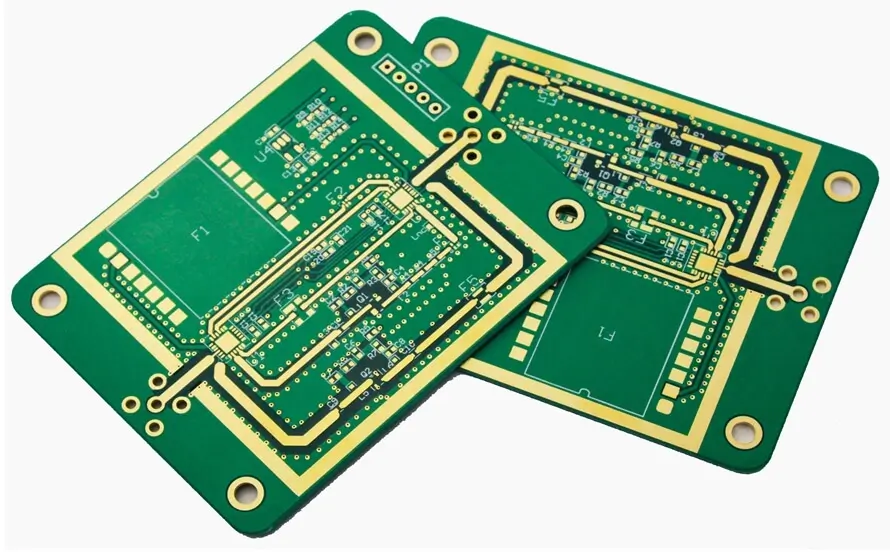
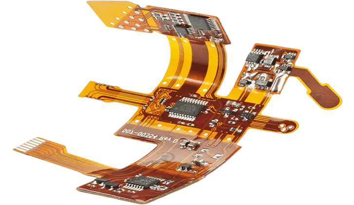
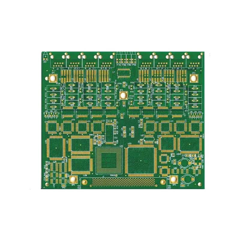
Rigid PCB
B.01
Rigid PCB
Standard FR4-based boards for general-purpose electronics. Single-sided, double-sided, and multilayer up to 12+ layers with controlled impedance.
FR4 / Rogers 1–12L 3 mil min track HASL / ENIG
Flexible PCB
B.02
Flexible PCB (FPC)
Polyimide-based flex circuits for space-constrained assemblies, wearables, and dynamic-bend applications. Single and double-layer flex.
Polyimide 1–2L Dynamic bend ZIF connectors
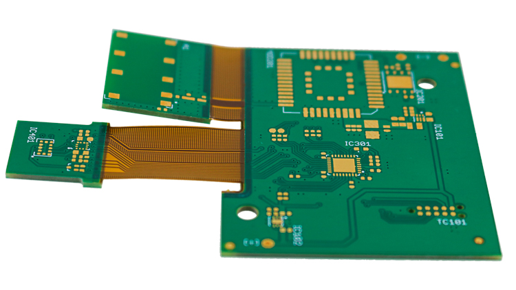
Rigid-Flex PCB
B.03
Rigid-Flex PCB
Combined rigid and flexible zones in a single board — eliminating connectors and reducing assembly cost for medical devices, aerospace, and industrial controls.
FR4 + Polyimide 4–8L Medical grade IPC-2223
Multilayer PCB
B.04
Multilayer PCB
4 to 12+ layer stackups with controlled impedance, buried vias, and blind vias. Designed for high-speed digital and mixed-signal applications.
4–12+ layers Blind / buried via 100Ω ±10% High-speed
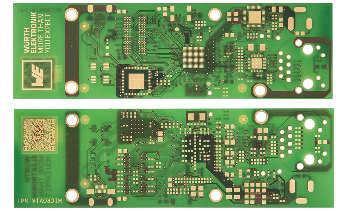
HDI Microvia PCB
B.05
HDI / Microvia
High-Density Interconnect boards with laser-drilled microvias for BGA fanout, advanced IC packages, and miniaturized consumer and medical electronics.
Laser via ≤0.1mm BGA fanout Any-layer HDI 0.4mm BGA pitch
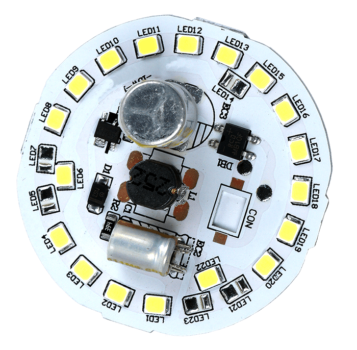
Metal Core PCB
B.06
Metal Core PCB (MCPCB)
Aluminum or copper-core substrates for high-power LED drivers, power electronics, and motor control applications requiring superior thermal management.
Al / Cu core 1–2L 1–3 W/m·K LED / Power
03 / Process

Ten stages. Zero guesswork.

Every project follows a structured workflow from requirements capture through packaged delivery — with customer visibility at each gate.

01
Requirements Capture
Schematic, BOM, mechanical envelope, and target application reviewed with your engineering team.
02
Schematic Review
Design rule check, net verification, and DFM recommendations before layout begins.
03
Layer Stackup
Dielectric selection, impedance targets, and via strategy confirmed per IPC-2141 and customer spec.
04
Component Placement
Thermal, EMI, and signal-integrity-driven placement with thermal pad and keepout zone compliance.
05
Routing & DRC
Manual and auto-route with impedance-controlled traces, differential pairs, and full design rule check sign-off.
06
Gerber Output
Customer-reviewed Gerbers, ODB++, drill files, assembly drawings, and fab notes released to fabrication partner.
07
Fabrication
Inner layer imaging, lamination, precision drilling, plating, outer layer patterning, soldermask, and surface finish.
08
SMT Assembly
Stencil printing, pick-and-place, reflow soldering, selective soldering for THT, and conformal coating on request.
09
Inspection & Test
AOI, flying-probe electrical test, ICT, and functional test executed per agreed test plan with full test records.
10
Delivery
ESD-safe packaging, CoC documentation, and same-country delivery to your facility — no customs delays.
04 / Services Detail

What we deliver at each stage.

D.01

PCB Layout & Design

Our engineers work from your schematic in Altium Designer, KiCad, or Eagle — producing a routed, DRC-clean layout optimized for your specific layer count, impedance requirements, and assembly process. We perform DFM review before releasing Gerbers, flagging component footprint issues, minimum annular ring violations, and solder mask slivers before they become fabrication problems.

For high-speed designs, we apply signal integrity analysis for differential pairs, length-matched data buses, and power delivery network decoupling — ensuring your board performs in production, not just in the lab.

  • Altium Designer, KiCad, Eagle — match your existing toolchain
  • Controlled impedance routing — 50Ω, 90Ω, 100Ω differential pairs
  • DFM review included — footprint, clearance, and assembly checks
  • Full Gerber package with assembly drawings and BOM cross-reference
  • Signal integrity analysis for DDR, PCIe, USB 3.x, and high-speed I/O
Design Capabilities
Min Track/Space3 / 3 mil
Min Via Drill0.2 mm
Max Layer Count12+
Board Thickness0.4 – 3.2 mm
Max Board Size500 × 600 mm
Surface FinishHASL, ENIG, OSP
EDA Tools: Altium Designer, KiCad 7, Eagle, Cadence Allegro (import/export). Deliverables include Gerber RS-274X, ODB++, IPC-2581, and native project files.
D.02

PCB Fabrication

We manage fabrication through qualified partner facilities with full IPC-6012 Class 2 and Class 3 capability. All substrates undergo incoming material inspection, and completed bare boards receive electrical continuity and isolation testing on flying-probe fixtures before leaving the fab.

For impedance-critical designs, we maintain controlled-impedance coupon testing on every panel, with TDR measurement reports included in the quality pack. Certificates of conformance and UL-marked laminates are available on request.

  • IPC-6012 Class 2 and Class 3 fabrication compliance
  • Flying-probe electrical test on every bare board
  • Impedance coupons with TDR reports for controlled-impedance boards
  • Surface finishes: HASL (lead-free), ENIG, OSP, immersion silver, hard gold
  • 48-hour express prototype with full quality documentation
Fabrication Specs
Prototype Lead Time48 – 72 hr
Production Lead Time5 – 10 days
Copper Weight0.5 – 6 oz
Aspect Ratioup to 10:1
SoldermaskLPI, any colour
SilkscreenBoth sides
Certifications available: IPC-6012, UL94-V0 laminate, RoHS-compliant process, IATF 16949 supply chain on request for automotive applications.
D.03

SMT & Through-Hole Assembly

Surface mount assembly from solder paste printing through reflow, covering 0201 passives, fine-pitch QFP, BGA, LGA, and CSP packages. Our assembly line operates under IPC-A-610 acceptance criteria, with AOI and X-ray inspection available for BGA and hidden-joint verification.

Through-hole components are processed via selective soldering or hand soldering per IPC-A-610. For mixed-technology boards, we coordinate the full process sequence to minimise thermal excursions on heat-sensitive components.

  • 0201 minimum component size — fine-pitch down to 0.4 mm BGA
  • AOI on every board, X-ray for BGA and LGA joints
  • Lead-free and leaded solder process available
  • Conformal coating (acrylic, silicone, urethane) for harsh environments
  • BOM procurement support and component sourcing from authorised distributors
Assembly Capabilities
Min Component0201 (0.6×0.3 mm)
Min BGA Pitch0.4 mm
Max Board Size450 × 500 mm
Placement Accuracy±30 µm
InspectionAOI + X-ray
IPC StandardIPC-A-610 Class 2/3
Turnkey or consignment: We can procure your BOM from authorised distributors, or assemble from customer-supplied components. Partial kitting also accepted.
05 / Quality Control

Six checkpoints. Zero escapes.

Every build passes through six independent inspection stages — each with documented records you can reference against your IPC audit requirements.

01

IQC — Incoming Quality Control

All components and bare boards inspected on receipt. Date codes, quantity, and package marking verified before kitting. Counterfeit screening available on request.

02

SPI — Solder Paste Inspection

3D solder paste volume, area, and offset measured at every deposit after printing. Boards failing SPI are re-printed — not sent to placement.

03

First Article Inspection

After placement, the first board of every job is manually verified by an engineer before the full run is approved. Component identity, polarity, and position confirmed against BOM.

04

AOI — Automated Optical Inspection

Post-reflow AOI detects missing components, solder bridges, lifted leads, tombstoning, and polarity errors with photographic evidence logged per board.

05

X-Ray — Hidden Joint Inspection

BGA and other hidden-joint packages inspected by X-ray for voiding, cold joints, and bridging not visible to AOI. Sampling rate or 100% inspection per your spec.

06

Final QA & Shipment Inspection

IPC-A-610 visual workmanship check by a certified IPC-CIS. CoC, test records, and traveller documentation packaged with every shipment.

06 / Testing Services

Test coverage for every build class.

From simple AOI to full functional validation — we match test coverage to your product's risk profile and qualification requirements.

AOI Testing
Automated optical inspection on every board post-reflow. Detects placement errors, bridges, and opens with full image archive.
X-Ray Inspection
BGA solder joint analysis — voiding percentage, bridging, and cold joints in hidden packages verified to IPC-7095 criteria.
In-Circuit Test (ICT)
Bed-of-nails fixture tests component values, opens, shorts, and basic function. Ideal for mid-to-high volume production boards.
Flying Probe
Fixtureless electrical test for prototype and low-volume builds. Checks opens, shorts, and component values without a dedicated ICT fixture.
Functional Test (FCT)
Board powered up and exercised through its operating modes using customer-supplied or Antech-developed test jigs and scripts.
IC Programming
Microcontroller and FPGA device programming during assembly. Firmware version controlled and verified post-programming before shipment.
Environmental Stress
Burn-in, thermal cycling, and humidity exposure for accelerated life testing. Supported by our QRA laboratory for full qualification packages.
Conformal Coating
Acrylic, silicone, or polyurethane coating applied to customer spec for protection against humidity, corrosion, and vibration.
07 / Component Sourcing

Kitted or turnkey — your choice.

Bring your own parts or let us source everything. Either way, every component goes through IQC before it touches your board.

Kitted Assembly

You supply the parts

You deliver pre-kitted components matched to your BOM
Antech performs incoming inspection on all supplied parts before assembly
Ideal when you have existing supplier relationships or approved vendor lists
Any shortages or discrepancies flagged before build commences — no surprises mid-run
Consigned and customer-owned inventory managed with barcode tracking
Turnkey Assembly

We source everything

BOM submitted — we quote and procure all components through authorised distribution channels
Date code and authenticity verified; counterfeit screening available for critical ICs
Rare and long-lead parts sourced through our regional supply chain network
Part crosses and approved substitutes offered with customer sign-off before procurement
Single invoice covers components and assembly — simplifies your PO process
08 / Why Antech

Single-source. Local engineers. No delays.

Most Philippine manufacturers juggle separate vendors for design, fabrication, and assembly. We combine all three under one roof, with engineers based in-country.

One Vendor, Full Cycle
Design, fabrication, and assembly managed from a single point of contact. No handoff errors, no finger-pointing between suppliers, and one purchase order covering the complete scope.
Responsive Engineering Support
Your design is handled by dedicated engineers available during your business hours — same-day feedback, fast design reviews, and direct access for change orders without queues or delays.
Local Stock, Fast Delivery
Common substrates, soldermask materials, and surface finish chemicals held in our Parañaque facility. No import lead time on standard materials — prototype boards within 48 hours of Gerber approval.
09 / FAQ

Common questions.

For layout design: schematic (PDF or native EDA file), BOM, and mechanical drawings. For fabrication only: Gerber RS-274X files, drill file (Excellon), and a readme with stackup and impedance requirements. For assembly: Gerbers, BOM with manufacturer part numbers, and centroid (pick-and-place) file. If you have an existing design but no Gerbers, we can extract them from your native files.

Yes. Our assembly line handles BGA down to 0.4 mm pitch and CSP packages. X-ray inspection is available for all hidden-joint verification. For HDI designs requiring laser-drilled microvias to fan out fine-pitch BGA, we coordinate with our fab partner for the appropriate any-layer HDI stackup.

We offer full turnkey (we source all components from authorised distributors — Avnet, Mouser, Digi-Key, or local PH distributors), partial kitting (you supply the long-lead or controlled components, we source the rest), and consignment assembly (you supply all components, we assemble). We do not purchase from grey-market or unverified brokers.

Yes. For automotive applications we support AEC-Q component selection guidance, IATF 16949-aligned supplier chain for fabrication, high-temperature laminates (Tg 170+), and extended IPC-A-610 Class 3 inspection criteria. We can generate PPAP documentation for your incoming quality records on request.

There is no minimum order quantity. We regularly run single-board prototypes for R&D teams and scale to production volumes of thousands of units for EMS customers. Pricing is naturally more economical at higher volumes, but we do not impose a minimum.

Start a project

Ready to build your next board?

Send us your schematic, Gerbers, or just a napkin sketch — our engineers will review your design and come back with a quote and DFM feedback, usually within one business day.